Examples and Libraries on the CBA Gitlab
An entry-point and beginner’s guide to circuit design.
Design
Schematics and Boards
No matter what software you’re using, it’s important to understand the two representations we use to describe circuits.
To jump in, I’ve included this example eagle project that you can clone (it will probably even work!) to see what-all is going on when you’re designing circuits.
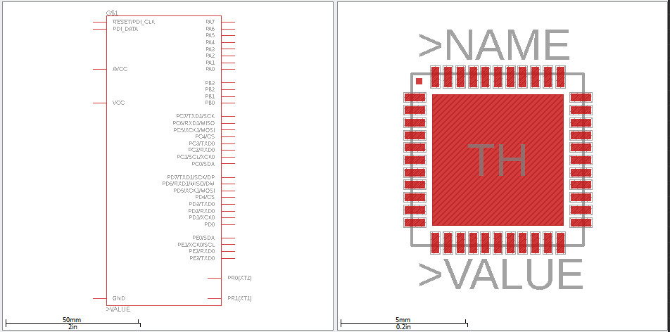
The schematic is a nonphysical space where we can describe which outputs or inputs from our various components are connected to one another. In a schematic, we find part symbols that pave pins, these are connected to one another on nets.
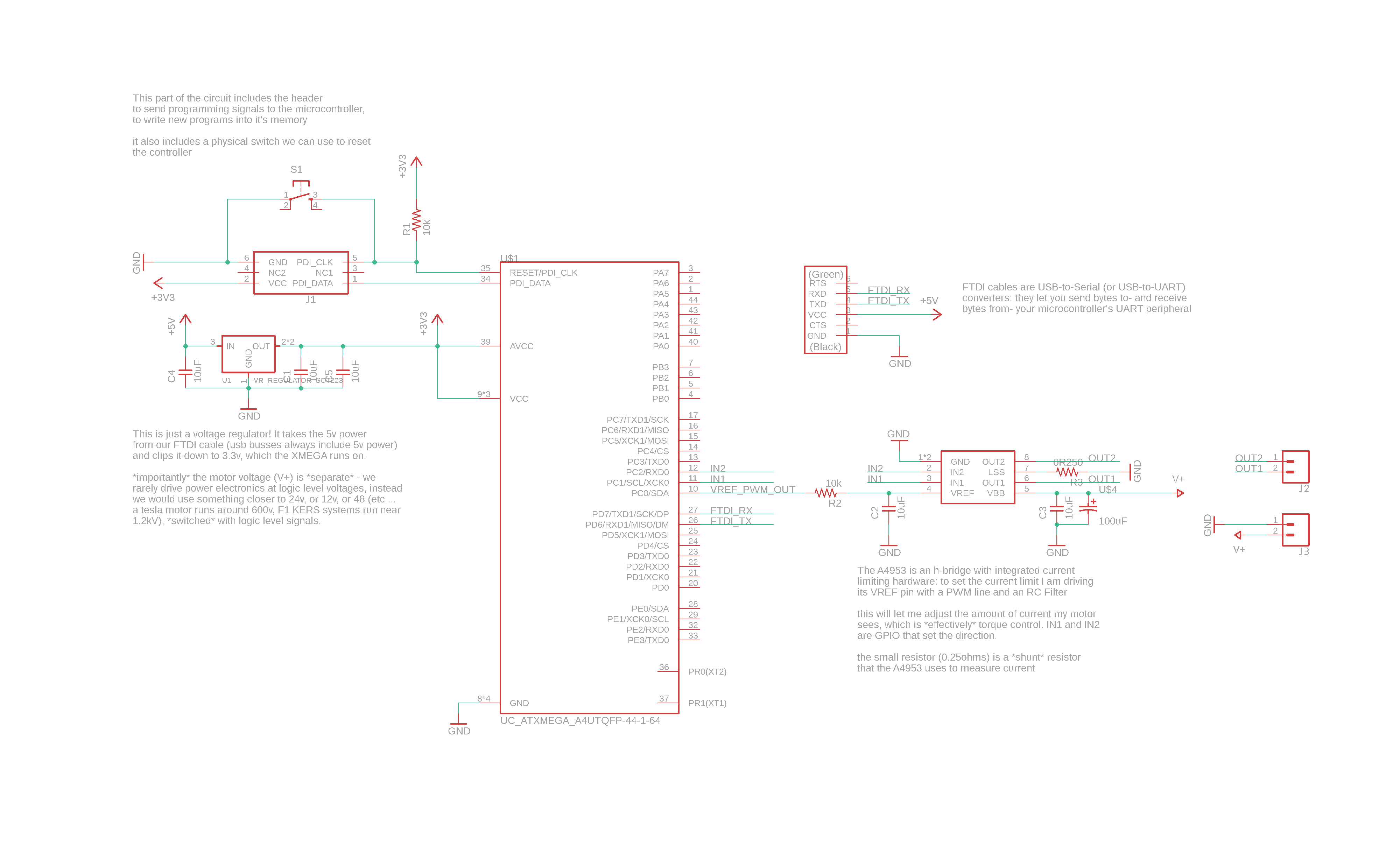
Critically, we can connect nets to one another by simply assigning them the same name. This is a useful trick that you will probably encounter many times in the wild. Also important to note are supply components, like the gnd and v+ or +3v3 etc symbols, which are simply symbolic representations of similarely named nets.
It’s not-not useful to recall that schematics are also nice visual diagrams of what we want our circuits to do. There’s no harm in making them look medium-nice. :bowtie:
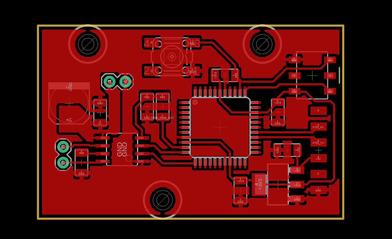
The board representation is where our design meets the physical world. Here we find footprints that have pads that are connected to one another via traces, vias, and pours i.e. copper.
In Eagle, boards and schematics should be automatically associated with one another. This is referred to as ‘forward/back annotation’ - but typically goes one way: from the schematic to the board. It’s best, while we’re starting, to treat this relationship as a directional one. I.E. when you’re deleting a component, do so in the schematic, otherwise you will introduce inconsistencies and Eagle might abandon you.
KiCAD uses a different system, where we save a netlist from our schematic, and open that in a board editor. This is partially an opinion about the division between the two practices, and partially a historic artefact of KiCAD’s development as a collection of not-unrelated softwares.
Symbols and Footprints
Our circuit assemblies are made of schematics that are diagrams of our boards, and so the components we use to put them together have a similar split; we call them symbols and footprints.
A symbol is a diagram of a part, and the footprint is the ‘landing’ that we need in order for the part to be successfully included in our circuit. The matching copper for us to hook the IC to.

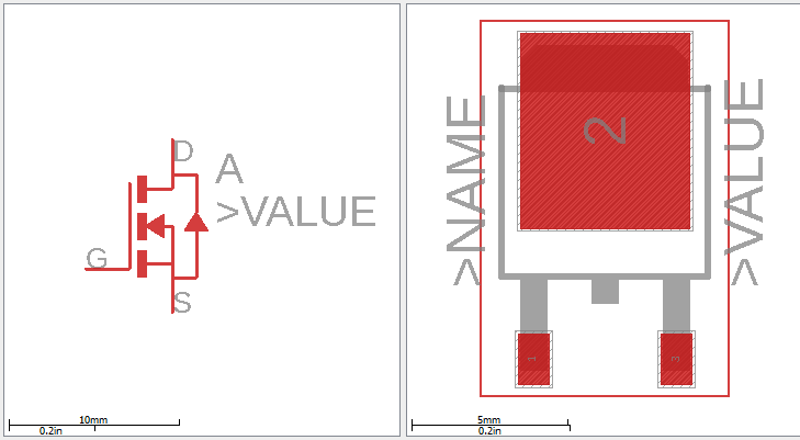
Symbols can have multiple footprints: the same or similar silicon divices can be packaged in varying sizes for circuit integration.
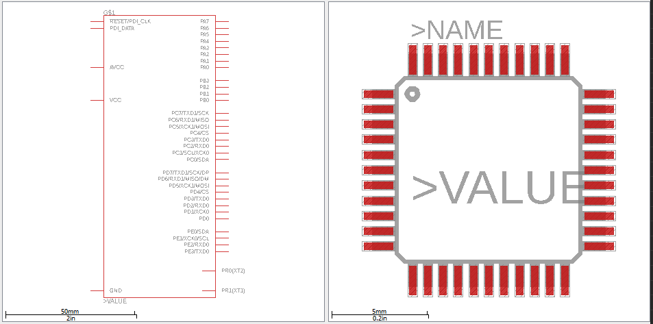
To make your own symbols or footprints, I can recommend Autodesk’s Tutorial, starting here and for KiCAD, the symbol, footprint, and the association.
Libraries
To organize collections of parts, we use libraries of devices: paired symbols and footprints. For eagle, I’ve included our CBA libraries in the eagle/parts directory of this repo. I’ve also included the sparkfun libraries as I commonly use their connectors library for pin-headers. Parts in the fablab library should all be available in fab labs, but it’s best to check with actual inventory before designing a circuit. It’s also likely that parts in the inventory are not yet in the library: if you find this to be the case, and you make a footprint for a part you would like to use (or find one online) please push a merge request, or raise an issue in this repo!
The fablab inventory includes all of the circuit components that should be available in the lab.
Manufacturing
Different methods of circuit manufacture have different constraints. We commonly call these design rules - they define a variety of things, the most important being the trace/space dimension: how thin can we make a trace, and how much gap must we leave between each different signal? The next important question is about how small our minimum drill size is: this sets the diameter of our vias.
For ‘most’ fabricators, a lenient (easy to fab) trace/space is 8/8mil (mil: 1/1000 of an inch: 8mil: 0.2032mm), with a 0.35mm minimum sized hole (that’s 13.8mil). For some reason, we commonly refer to ‘mil’ for traces and mm for holes. The world is full of idiosyncrasies. Fabricators who can’t do this are really, really not worth the time.
For the circuit milling we do in the lab, we set our space by the width of our end-mills: the 1/64th endmills are 15.625mil in diameter, so for some error band I use a 16mil space, and to avoid accidentally milling traces away, I typically set a 12mil trace. 12/16 means it is occasionally difficult to mill footprints for newer component packages like a QFN. Drilling holes under 1/32” is also a pain, so I’ll normally set my minimum drill to 32mil.
In any case, if you’d rather not think about any of this, I’ve included some Eagle design rules files in this repo in the eagle/design-rules folder. You can load these into eagle in the board-design window through edit >> design rules, or the drc command. Once you’ve done this, you can run the ‘drc’ command to check if your design violates any of the rules.
TODO: want to keep a list of manufacturer design-rules files or board templates (grid etc) for two- and four- layer fab at factory.
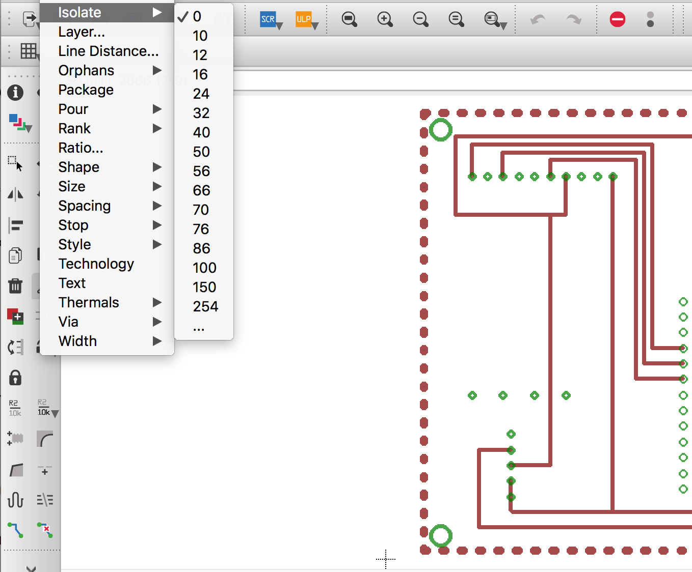
Automating the generation of trace.png and cutout.png files
Matt Keeter wrote a Python script that opens up Eagle and exports a number of pngs using ImageMagick. Last I know, this is tested for Eagle 7- or 8.
To get this script to run, use the following steps:
- Save eagle/scripts/eagle_png.py into the folder where you keep your Eagle project folders containing .brd and .sch files
- Install ImageMagick
- Create a polygon over your .brd design on the Milling layer (number 46)
- Set the isolate value for the polygon to a number greater than 16, this will ensure there’s enough black space for mods to generate toolpaths in (see image below)
- Save your .brd file and close Eagle
- Run eagle_png using the following command
python eagle_png.py board_folder/board_name.brd - The script should have saved several .png files into the folder where the .brd file is
Note: With later versions of Eagle (9.0.1+), by default it is configured to show text similar to “1-16” ontop of each via. This comes through even when exporting your final image. To remove this artifact, type the following in the commandline:
SET Option.ViaLength 0
SMT (board house) Manufacture
Adafruit already has some great notes on SMT manufacturing.
L1: boardfab, solder by hand
Export
Making Gerbers
L2: paste, stencils, and tweezers
L3: diy pnp
L4: circuit assembly
For assembly, some miters tips are
- circuithub
- lightspeed manufacturing (in MA)
- tempo automation
- maybe worth trying jlc/easyeda - just have to constrain boards to parts they have (probably)